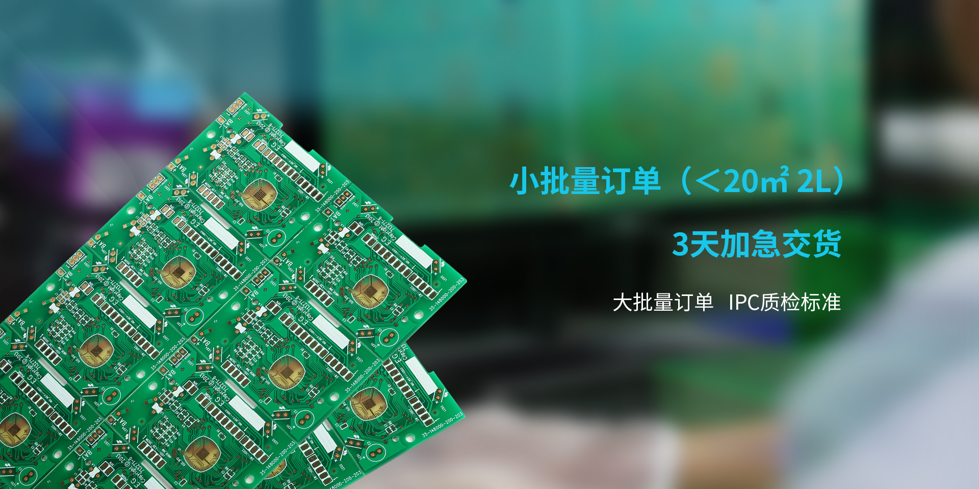
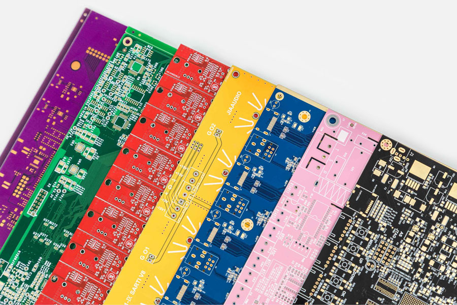
Customization Center
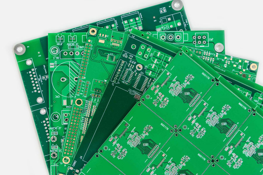
- circuit board
- Power circuit board
- Industrial control circuit board
- Security circuit board
- Medical circuit board
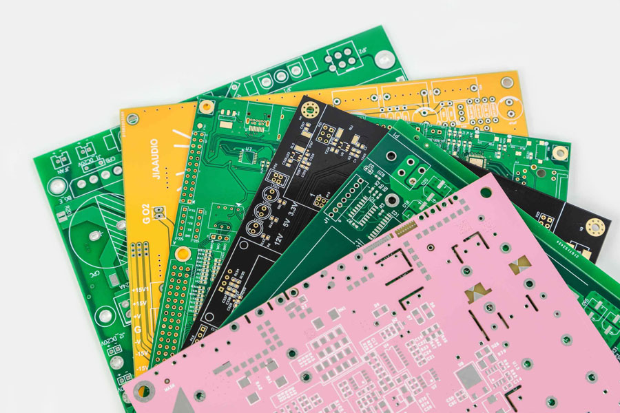
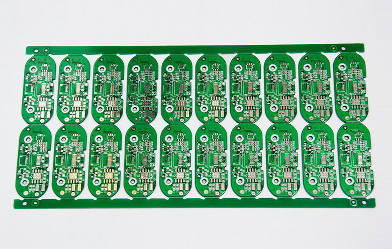
circuit board
Base material: FR4-S1000-2M
Plate thickness: 1.6mm
Number of layers: double-sided board
Process: lead-free tin spraying
Minimum drilling hole: 0.25mm
Minimum line width: 0.1mm
Minimum line spacing: 0.1mm
Features: Strict appearance requirements, line width and distance of 4mil
Power circuit board
Substrate: FR4
Plate thickness: 1.6mm
Number of layers: double-sided board
Process: lead-free tin spraying
Minimum drilling hole: 0.3mm
Minimum line width: 0.16mm
Minimum line spacing: 0.16mm
Features: High current, high reliability, thick copper plate
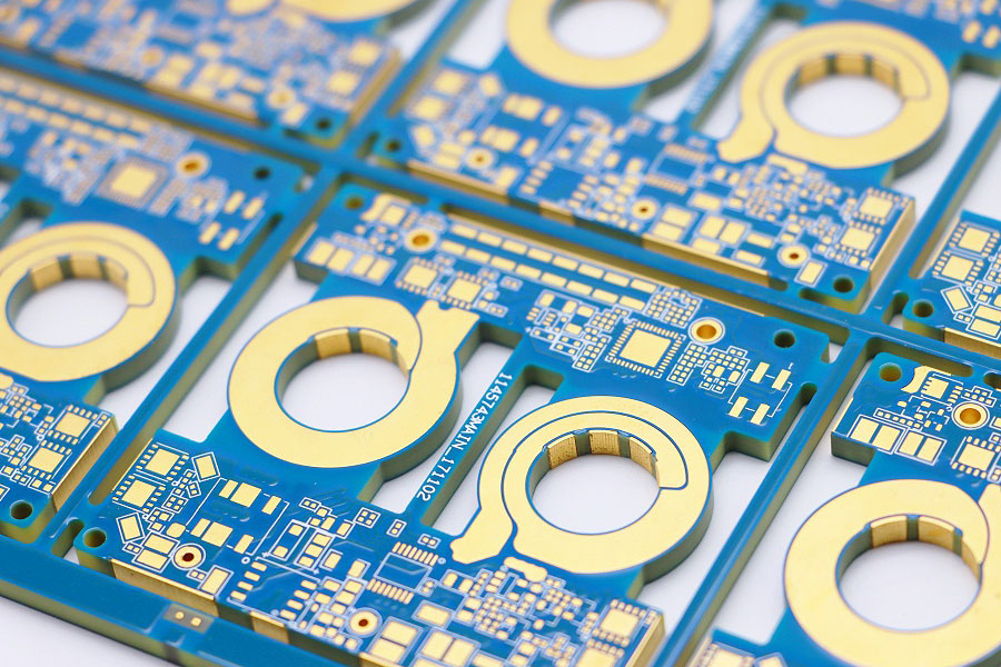
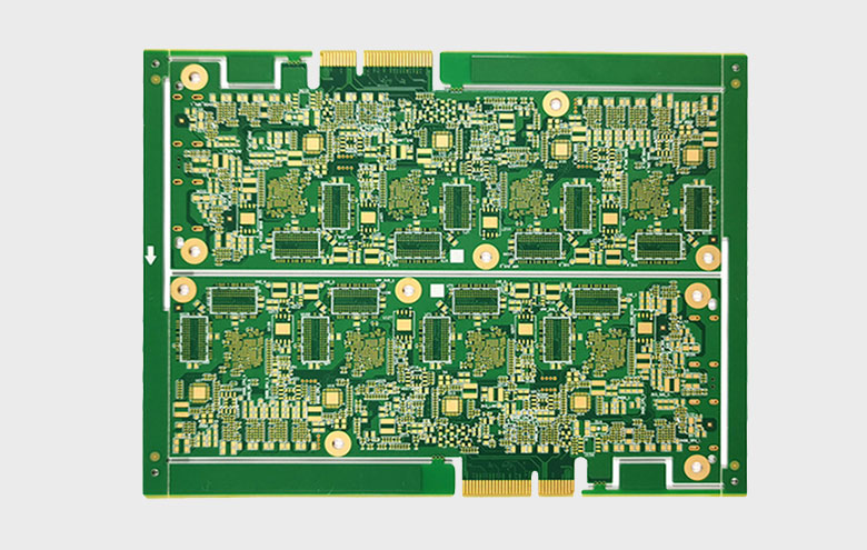
Industrial control circuit board
Base material: FR4-S1000-2M
Plate thickness: 1.6mm
Number of layers: four layer board
Process: Sinking Gold Plate
Minimum drilling hole: 0.25mm
Minimum line width: 0.16mm
Minimum line spacing: 0.16mm
Features: Gold finger, impedance board, gold finger requires beveled edges
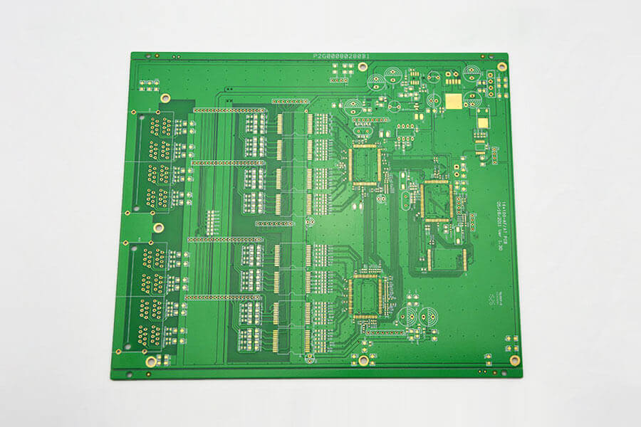
Security circuit board
Base material: FR4-S1000-2M
Plate thickness: 1.6mm
Number of layers: Six layers of board
Craft: Sinking Gold+Gold Fingers
Minimum drilling hole: 0.25mm
Minimum line width: 0.1mm
Minimum line spacing: 0.1mm
Features: Hole copper 25um, thick copper plate, internal and external 4oz, blind buried hole plate
Medical circuit board
Substrate: FR4
Plate thickness: 1.6mm
Number of layers: double-sided board
Process: gold-plated plate
Minimum drilling hole: 0.25mm
Minimum line width: 0.1mm
Minimum line spacing: 0.1mm
Features: High level PCB, impedance board, and through hole plug holes are not allowed to turn red